
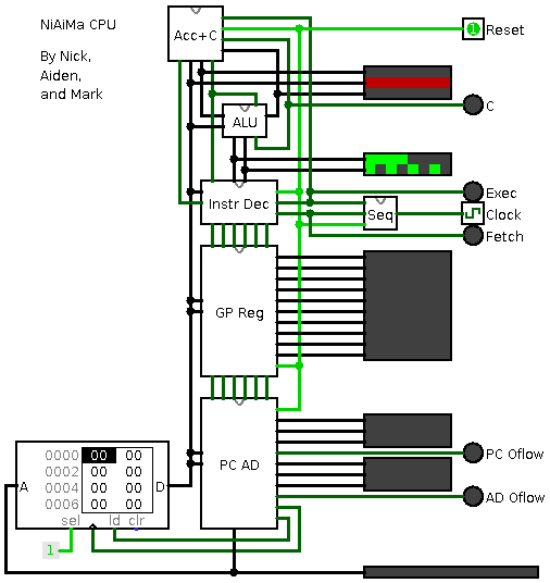
Whilst watching Harry Porter's relay CPU we thought that designing our own CPU would be fun. A while later we found a program called Logisim that could simulate logic gates, with hierarchical logic blocks, allowing you to make your own building blocks and re-use them in increasingly complicated circuits. Over the next few weeks we used Logisim to design and simulate an 8-bit RISC CPU - that's what we do for fun!
All instructions have a single Fetch / Execute cycle. The ALU "A" input is always connected to a register called the Accumulator. The ALU outputs to the accumulator as well, for use in the next instruction cycle(s). A single carry/condition bit is similarly kept from each instruction for future instruction cycles. We have 10 general-purpose registers, any of which can be used as the "B" input to the ALU. Some instructions write. Some special-purpose registers can be treated as 16-bit address registers used to read/write memory, with auto post-increment and pre-decrement. One pair is used as a Program Counter (PC), the other is an indirect address register (AD) often used as a stack pointer. Most instructions have 4 bits of "Operation" and 4 bits used to select the register to be read/written. Some simpler instructions only work on the Accumulator and Carry.
We named our CPU after the first 2 letters of each of our names - Nick (dad), Aiden, and Mark (13-year old twins)
We started with an 8-bit ALU that could do any simple boolean instruction you like, add, subtract, and a few other ripple-carry operations
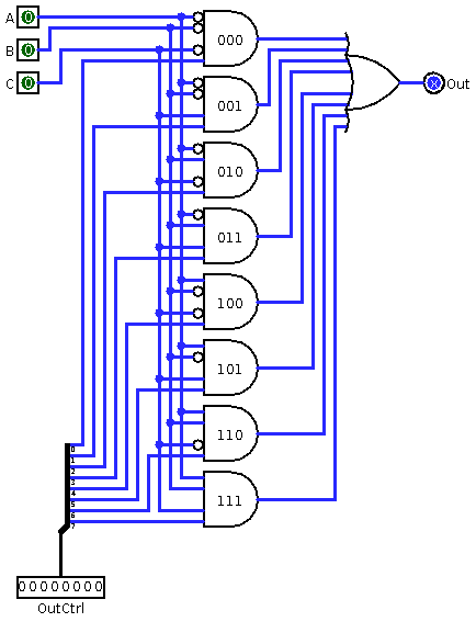
Our 1-bit "AnyLogic" gate takes 3 inputs, A, B, C, and an 8-bit control. It acts as any 3-input, 1-output logic gate, for example:
| A in | 1 | 1 | 1 | 1 | 0 | 0 | 0 | 0 |
|---|---|---|---|---|---|---|---|---|
| B in | 1 | 1 | 0 | 0 | 1 | 1 | 0 | 0 |
| C in | 1 | 0 | 1 | 0 | 1 | 0 | 1 | 0 |
| Out | 1 | 0 | 0 | 0 | 0 | 0 | 0 | 0 |
Here we are showing the logic operation "A and B and C". The output is 1 only if A and B and C are all 1. We can perform this in our AnyLogic gate with the Control input set to 10000000 - the values you see in the bottom row. Some other interesting operations are:
| A | 1 | 1 | 1 | 1 | 0 | 0 | 0 | 0 |
|---|---|---|---|---|---|---|---|---|
| B | 1 | 1 | 0 | 0 | 1 | 1 | 0 | 0 |
| C | 1 | 0 | 1 | 0 | 1 | 0 | 1 | 0 |
| A and B and C | 1 | 0 | 0 | 0 | 0 | 0 | 0 | 0 |
| A and B (ignore C) | 1 | 1 | 0 | 0 | 0 | 0 | 0 | 0 |
| A or B or C | 1 | 1 | 1 | 1 | 1 | 1 | 1 | 0 |
| A or B (ignore C) | 1 | 1 | 1 | 1 | 1 | 1 | 0 | 0 |
| A xor B xor C | 1 | 0 | 0 | 1 | 0 | 1 | 1 | 0 |
| Not A | 0 | 0 | 0 | 0 | 1 | 1 | 1 | 1 |
| Not B | 0 | 0 | 1 | 1 | 0 | 0 | 1 | 1 |
| A+B+C (carry) | 1 | 1 | 1 | 0 | 1 | 0 | 0 | 0 |
| A+B+C (out) | 1 | 0 | 0 | 1 | 0 | 1 | 1 | 0 |
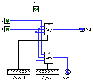
By combining 2 of our "AnyLogic" gates, we make a 1-bit ALU. We treat A and B as regular inputs, C as a carry input, one "AnyLogic" produces out output bit, another "AnyLogic" produces the carry output to be sent to the next stage.
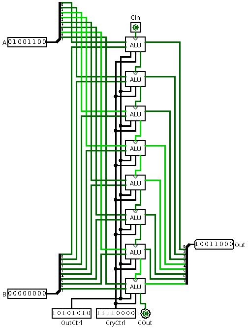
8 of these 1-bit ALUs are arrange into an 8-bit ALU. The A and B inputs are now regular 8-bit inputs, combined to form an 8-bit output. The single-bit Carry input "CIn" is rippled from the lowest bit to the highest bit, and then output. When adding, C can be used as a Carry, obviously, but some other operations can use it as a flag, for example we use C to choose whether to output A or B - if C is set (1) we output A, if C is clear (0) we output B:
| A | 1 | 1 | 1 | 1 | 0 | 0 | 0 | 0 |
|---|---|---|---|---|---|---|---|---|
| B | 1 | 1 | 0 | 0 | 1 | 1 | 0 | 0 |
| C | 1 | 0 | 1 | 0 | 1 | 0 | 1 | 0 |
| If C then A else B | 1 | 1 | 1 | 0 | 0 | 1 | 0 | 0 |
| C out | 1 | 0 | 1 | 0 | 1 | 0 | 1 | 0 |
We have to keep the Carry (/condition) value all the way down the 8-bit ALU otherwise this would only work on the first (lowest) bit.
We can also perform a "Shift Left" operation, by using the Carry to pass each input bit 1 place left. We ignore B. We output the "carry in", and we set the next carry to be the A bit:
| A Input | |||||||||
|---|---|---|---|---|---|---|---|---|---|
| 7 | 6 | 5 | 4 | 3 | 2 | 1 | 0 | ||
| Cout |  |
 |
 |
 |
 |
 |
 |
 |
CIn |
| 6 | 5 | 4 | 3 | 2 | 1 | 0 | C | ||
| Output | |||||||||
| A | 1 | 1 | 1 | 1 | 0 | 0 | 0 | 0 |
|---|---|---|---|---|---|---|---|---|
| B | 1 | 1 | 0 | 0 | 1 | 1 | 0 | 0 |
| C | 1 | 0 | 1 | 0 | 1 | 0 | 1 | 0 |
| Out | 1 | 0 | 1 | 0 | 1 | 0 | 1 | 0 |
| C out | 1 | 1 | 1 | 1 | 0 | 0 | 0 | 0 |
We can't perform a "Shift Right", because our carry always goes left not right, but we are also shifting C in, and out to C, so could perform a right-shift by doing 8 left-shifts:
| 0 shifts | 7 | 6 | 5 | 4 | 3 | 2 | 1 | 0 | C |
|---|---|---|---|---|---|---|---|---|---|
| 1 shift | 6 | 5 | 4 | 3 | 2 | 1 | 0 | C | 7 |
| 2 shifts | 5 | 4 | 3 | 2 | 1 | 0 | C | 7 | 6 |
| 3 shifts | 4 | 3 | 2 | 1 | 0 | C | 7 | 6 | 5 |
| 4 shifts | 3 | 2 | 1 | 0 | C | 7 | 6 | 5 | 4 |
| 5 shifts | 2 | 1 | 0 | C | 7 | 6 | 5 | 4 | 3 |
| 6 shifts | 1 | 0 | C | 7 | 6 | 5 | 4 | 3 | 2 |
| 7 shifts | 0 | C | 7 | 6 | 5 | 4 | 3 | 2 | 1 |
| 8 shifts | C | 7 | 6 | 5 | 4 | 3 | 2 | 1 | 0 |
| 9 shifts | 7 | 6 | 5 | 4 | 3 | 2 | 1 | 0 | C |
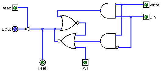
Logisim has a few types of registers built in, but we decided we wanted to do it ourselves from scratch. When Write is active, one of the 2 NOR gates gets powered, allowing the other to lock them in place. The loop of back-to-back NOR gates is either locked on/off, or off/on. We can read from this loop as a "Peek" (any time) or a real "Read" which pulls a tristate high or low. We can also reset ("RST").
The animated register here is demonstrating writing a zero, reading it, writing a 1, reading it, and repeating. Hover over it to reset (RST), which forces a 0 to be written.
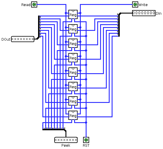
We combine 8 of these to make an 8-bit register.

Our registers have "active high" Write inputs, they are not edge-triggered, so we need two 8-bit registers for our Accumulator. One holds the current accumulator value, the other latches the next value on execute cycles. Our Carry logic is the same but only 1-bit.
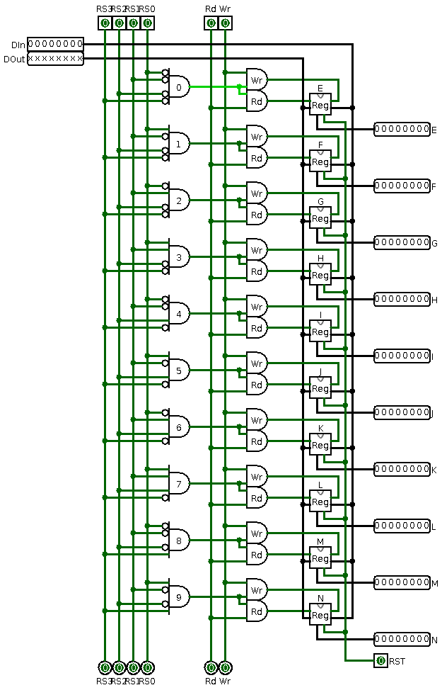
Our CPU has 16 addressable registers. 10 of them are General-purpose registers. We select a register using RS3/2/1/0 through the AND gates, then Read (Rd) onto the data bus (DOut) or Write (Wr) from the data bus (DIn). We named these registers E to N. The "Peek" outputs are output just to be displayed on LEDs (see later).
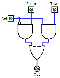
Again we could have used Logisim built-in blocks but wanted to create our own: A 1-bit "Mux" is made from 3 logic gates. It uses a "Sel" input to choose between "False" and "True" inputs.
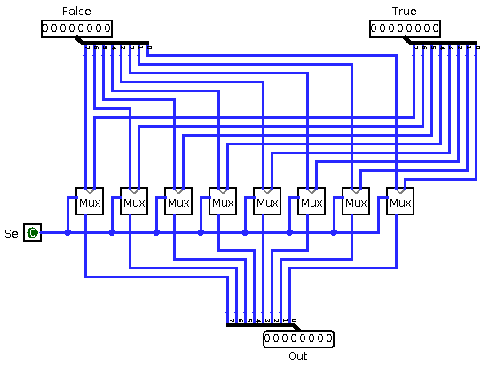
8 are combined for an 8-bit mux where an 8-bit output is Selected from one of the two 8-bit inputs.
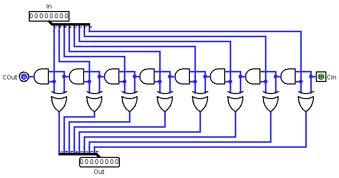
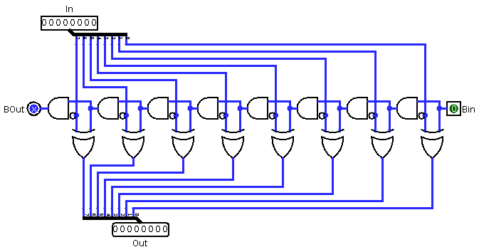
Some of our special-purpose registers will need to self-increment or decrement without using the ALU. The circuits here perform a simple ripple-carry increment ("add one") or decrement ("subtract one")
Unlike our "active high" registers, Logisim's RAM is rising-edge triggered, so it sometimes reads (or worse, writes) errors whilst our logic is still settling, unless we deliberately delay "memory write" by about 10 gate-delays.
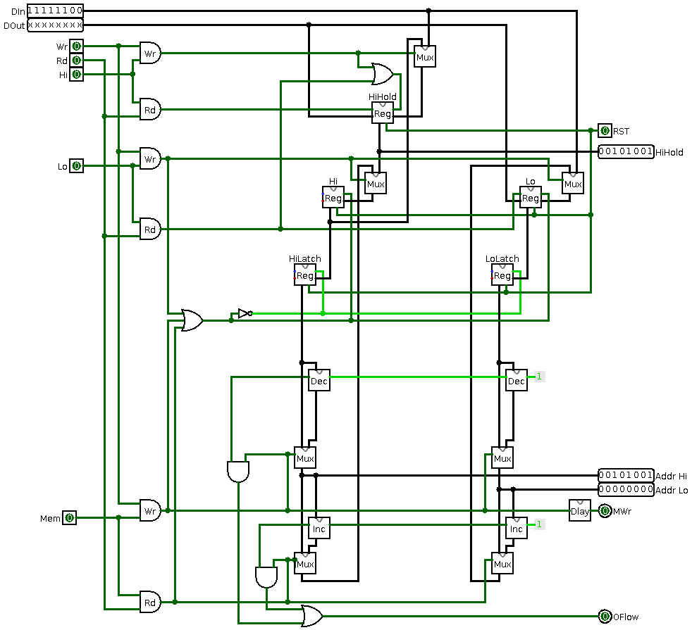
Our CPU also has some special-purpose registers. A pair of 8-bit registers acts as the Program Counter (PC) where our instructions are read, and they need to be used as a 16-bit address. After reading an instruction, our incrementor increments the values in the PC ready to read the next instruction. A similar pair acts as an ADdress register for stack and other memory operations. Before you write to the memory, they decrement. This will make stack operations possible, where we decrement and write to the stack pointer, or read and increment:
| A stack with 3 items: | dec and write (4th): | or read (3rd) and inc: | |||||
| ... | ... | ... | |||||
| ... | 4th | ←AD | ... | ||||
| 3rd | ←AD | 3rd | (3rd) | ||||
| 2nd | 2nd | 2nd | ←AD | ||||
| 1st | 1st | 1st | |||||
| ... | ... | ... | |||||
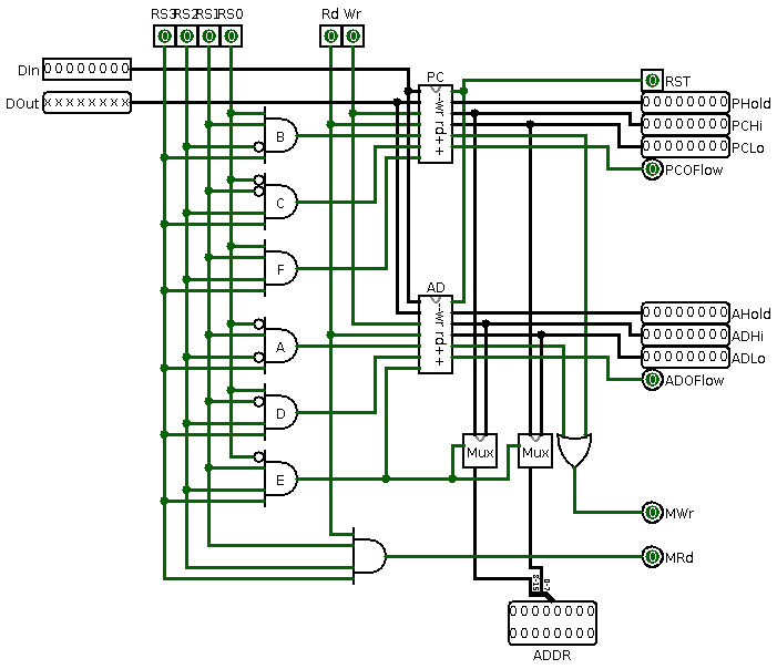
Each pair of registers consumes 3 "register select" values. One for the "high byte" (P in PC, or A in AD), one for the "low byte" (C in PC, or D in AD), and one for memory read/writes using PC or AD as the address, with post=increment or pre-decrement.
The PC is almost always used in the "read and increment" mode, either during the Fetch cycle, and/or during the Execute cycle if we are using the register "[PC++]" (1111) - sort of an "immediate" addressing mode. To do a JUMP instruction, we write to the PC, but because we can only write 8 bits at a time, if we started by writing to P, then we would jump to an unintended location. We have something called "P holding" that gets written to P when we write to C. Similarly because we can't read P and C at the same time, we arrange for "Read C" to also transfer P into "P holding", which is what we actually read when we "Read P". This allows us to act as though we can read/write PC in one single operation even though in practice it will take 4 (FETCH a location, STORE to P (actually P-holding), FETCH another location, STORE to C, at which point P-holding is also written to P and we JUMP).
AD also has an "A holding" that holds a value to go into A when we write to D, or holds the value of A when we read D.
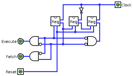
Hover over the image to reset our sequencer. Our sequencer uses a 3-bit shift register to create non-overlapping "Fetch" and "Execute" cycles. The sequence operates like:
| Clock | Reg | Output |
|---|---|---|
| 0 | 000 | |
| 1 | 001 | (*) |
| 0 | 011 | Fetch |
| 1 | 110 | |
| 0 | 100 | Execute |
| 1 | 001 | (see * above) |
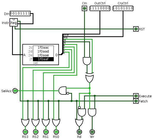
We used to decode the top 4 bits (for 16 instructions), using the lower 4 bits as "source/target register", however we we noticed a number of instructions that don't use a register, they operate only on the Accumulator and Carry/Condition flag. We instead decided to decode the full 8 bits using a ROM, though for many instructions we now repeat them 16 times, for the same instruction, but operating on each of the 16 registers.
During the fetch cycle, we select (RS) register 1111 - [PC++], and Read it into our Instr Register. This is then used as the address into a 256-row ROM. The outputs of the ROM are 8 bits of ALU output control, 8 bits of ALU Carry control, 2 bits of "Write select", 4 bits of register select (often, but not always, equal to the lower 4 bits of the Instruction Register).
The "Write Select" bits allow us to READ (00) from a register, Write (01) to the register, conditionally write (10) if Carry/Condition is 1, or conditionally write (11) if Carry/Condition is 0 (not yet used)
Our instruction set is shown below. For example, 59 is the "ADD N" instruction. The microcode 096e89 is in the ROM at address 0x59, decoded as WOOCCR where W=0, OO=96, CC=e8, R=9:
| Instruction | X0 | X1 | X2 | X3 | X4 | X5 | X6 | X7 | X8 | X9 | Xa | Xb | Xc | Xd | Xe | Xf |
|---|---|---|---|---|---|---|---|---|---|---|---|---|---|---|---|---|
| 0X | 0f0aa0 NOP |
0aaf00 SHL |
0f0000 CCLR |
0f0ff0 CSET |
0f00a0 IfZ |
0f0fa0 IfNZ |
0f0f00 IfNeg |
0f00f0 IfPos |
0aa000 CONE |
0aaaa0 CFF |
00faa0 INV |
05aaa0 CINV |
05aa00 CINC |
05a0a0 CDEC |
0a50a0 NEG |
000aa0 0 |
| 1X | 0ccaa0 FETCH |
0ccaa1 FETCH |
0ccaa2 FETCH |
0ccaa3 FETCH |
0ccaa4 FETCH |
0ccaa5 FETCH |
0ccaa6 FETCH |
0ccaa7 FETCH |
0ccaa8 FETCH |
0ccaa9 FETCH |
0ccaaa FETCH |
0ccaab FETCH |
0ccaac FETCH |
0ccaad FETCH |
0ccaae FETCH |
0ccaaf FETCH |
| 2X | 1f0aa0 STORE |
1f0aa1 STORE |
1f0aa2 STORE |
1f0aa3 STORE |
1f0aa4 STORE |
1f0aa5 STORE |
1f0aa6 STORE |
1f0aa7 STORE |
1f0aa8 STORE |
1f0aa9 STORE |
1f0aaa STORE |
1f0aab STORE |
1f0aac STORE |
1f0aad STORE |
1f0aae STORE |
1f0aaf STORE |
| 3X | 2d8aa0 CSTORE |
2d8aa1 CSTORE |
2d8aa2 CSTORE |
2d8aa3 CSTORE |
2d8aa4 CSTORE |
2d8aa5 CSTORE |
2d8aa6 CSTORE |
2d8aa7 CSTORE |
2d8aa8 CSTORE |
2d8aa9 CSTORE |
2d8aaa CSTORE |
2d8aab CSTORE |
2d8aac CSTORE |
2d8aad CSTORE |
2d8aae CSTORE |
2d8aaf CSTORE |
| 4X | 0e4aa0 ELSE |
0e4aa1 ELSE |
0e4aa2 ELSE |
0e4aa3 ELSE |
0e4aa4 ELSE |
0e4aa5 ELSE |
0e4aa6 ELSE |
0e4aa7 ELSE |
0e4aa8 ELSE |
0e4aa9 ELSE |
0e4aaa ELSE |
0e4aab ELSE |
0e4aac ELSE |
0e4aad ELSE |
0e4aae ELSE |
0e4aaf ELSE |
| 5X | 096e80 ADD |
096e81 ADD |
096e82 ADD |
096e83 ADD |
096e84 ADD |
096e85 ADD |
096e86 ADD |
096e87 ADD |
096e88 ADD |
096e89 ADD |
096e8a ADD |
096e8b ADD |
096e8c ADD |
096e8d ADD |
096e8e ADD |
096e8f ADD |
| 6X | 0968e0 SUB |
0968e1 SUB |
0968e2 SUB |
0968e3 SUB |
0968e4 SUB |
0968e5 SUB |
0968e6 SUB |
0968e7 SUB |
0968e8 SUB |
0968e9 SUB |
0968ea SUB |
0968eb SUB |
0968ec SUB |
0968ed SUB |
0968ee SUB |
0968ef SUB |
| 7X | 0c0ea0 AND |
0c0ea1 AND |
0c0ea2 AND |
0c0ea3 AND |
0c0ea4 AND |
0c0ea5 AND |
0c0ea6 AND |
0c0ea7 AND |
0c0ea8 AND |
0c0ea9 AND |
0c0eaa AND |
0c0eab AND |
0c0eac AND |
0c0ead AND |
0c0eae AND |
0c0eaf AND |
| 8X | 0fcfe0 OR |
0fcfe1 OR |
0fcfe2 OR |
0fcfe3 OR |
0fcfe4 OR |
0fcfe5 OR |
0fcfe6 OR |
0fcfe7 OR |
0fcfe8 OR |
0fcfe9 OR |
0fcfea OR |
0fcfeb OR |
0fcfec OR |
0fcfed OR |
0fcfee OR |
0fcfef OR |
| 9X | 03c960 XOR |
03c961 XOR |
03c962 XOR |
03c963 XOR |
03c964 XOR |
03c965 XOR |
03c966 XOR |
03c967 XOR |
03c968 XOR |
03c969 XOR |
03c96a XOR |
03c96b XOR |
03c96c XOR |
03c96d XOR |
03c96e XOR |
03c96f XOR |
| Read | E | F | G | H | I | J | K | L | M | N | A' | P' | (P→P')C | (A→A')D | [AD++] | [PC++]) |
| Register | (of AD) | (of PC) | (of PC) | (of AD) | (indirect) | |||||||||||
| Write | A' | P' | (P'→P)C | (A'→A)D | [--AD] | [--PC] | ||||||||||
The full contents of our Instruction Decoding ROM, including comments discussing the details of each command, register names, and possible (bits of) future commands, can all be downloaded. Most of the file is comments, only the "0f0aa0" hex strings without #s will be loaded into the Instruction Decoding ROM.
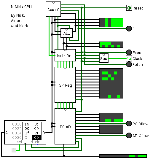
Now that we have everything described, we can build the entire CPU. The Accumulator and Carry/Condition sits just above the ALU so that there is less wiring. Below it is the Instruction Decoding, to control the ALU. The Sequencer, next to the Instruction Decoding, clocks throough the Fetch / Execute cycle. The General Purpose Registers sit below the Instruction Decoding, which selects a register and controls the Read / Write lines. Below that we placed the PC and AD Special-Purpose registers. PC (usually, AD occasionally) is output onto the address bus at the bottom, to control the RAM in the bottom-left. The Data bus sits to the left of the ALU, Instr Dec, GP Reg, and PC/AD. In the top right is the reset switch. Most of the rest on the right-hand side are blinky LED displays showing the values of all the registers and some control lines.
The entire Logisim circuit file NiAiMa.circ can be downloaded.
The image here shows the CPU after it has finished the multiplication of 42 * 100 to get 4200. multiply.hex can also be downloaded. This was our first real program for the NiAiMa CPU unless you count a few simple tests.
Our ALU can't multiply directly, so we made a program about 50 bytes long which does binary long-multiplication. 42 is stored in E. 100 is stored in F. G and H will store the 16-bit result. We do the long-multiplication by looping I=8 times for the 8 bits in E. We shift GH left (the "result so far"). We shift E left, setting Carry if it overflowed. If it did, we add F to GH, then we decerement our loop counter (I) and loop back. E is destroyed in the process by left-shifting it out, F is still 100, GH contains 1068 hex, which is 4200 decimal. M and N were used to store the "loop start" which can be (conditionally) written back to PC to jump back there.
[See Endianness on Wikipedia]. At this stage, our CPU is neither big-endian nor little-endian. Everything is 8-bit. There are no 16-bit or 32-bit instructions. 16-bit or 32-bit maths requires multiple commands, it usually makes sense to start at the 1s (Least Significant Byte - LSB) so you can carry into the next byte(s), but in memory we could store them in any order we like.
Some exceptions...
The examples above are very simple, just storing return addresses. Real stacks have areas for local variables, function parameters, and return values, often of different sizes. Rather than just having one Stack Pointer, there is sometimes a pointer called a Frame Pointer which only moves during calls/returns. The Frame Pointer points at the start of the frame for this current function. All local variables, arguments, temporary variables, return values are stored at known offsets from the Frame Pointer.
Because our AD register is also used for reading/writing any other part of memory, we can't always use it as a stack pointer. Instead we will use the MN registers as a Frame Pointer except during real stack operations (at some known offset of the Frame Pointer)
Ignore the terrible type errors, that's not the point. Also assume int=short=16bit for this example
// An example C program:
int main(int argc, char **argv) {
  byte X = foo(1,2,3);
  return 42 + X;
}
byte foo (int A, int B, int C) {
  byte D = bar(A, B);
  D     += bar(D,C);
  return D;
}
int bar(int X, int Y) {
  return X + Y;
}
When inside bar(), our stack might look like:
| hi | ptr | bar's stored frame ptr from foo() | ← Frame ptr [MN] whilst inside bar() |
| lo | |||
| hi | ptr | bar's return PC address (in foo()) | |
| lo | |||
| hi | int | bar's arg Y | |
| lo | |||
| hi | int | bar's arg X | |
| lo | |||
| hi | int | bar's return value | |
| lo | |||
| byte | foo's var D | ||
| hi | ptr | foo's stored frame ptr from main() | ← Frame ptr [MN] whilst inside foo() |
| lo | |||
| hi | ptr | foo's return PC address (in main()) | |
| lo | |||
| hi | int | foo's arg C | |
| lo | |||
| hi | int | foo's arg B | |
| lo | |||
| hi | int | foo's arg A | |
| lo | |||
| byte | foo's return value | ||
| byte | main's var X ( = foo's return value? ) | ||
| hi | ptr | main's stored frame ptr from OS? | ← Frame ptr [MN] whilst inside main() |
| lo | |||
| hi | ptr | main's return PC address? (OS somewhere?) | |
| lo | |||
| hi | ptr | main's argv | |
| lo | |||
| hi | int | main's argc | |
| lo | |||
| hi | int | main's return val | |
| lo | |||
| ... OS? ... | |||